ELECTRICAL AND RF
Design That Works the First Time
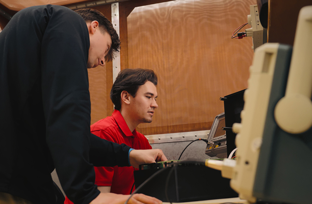
Thirty years and thousands of completed projects means we’ve seen most electrical and RF problems before they show up on the bench. Our engineers handle everything from power supplies to custom wireless protocols and antenna design. We do it in a facility where the electrical engineer creating your schematic sits twenty feet from the person designing the PCB layout.

What We Design

Digital and Embedded Systems
Microcontroller, microprocessor, and DSP based designs, using chip-down or system-on-module custom carrier board architectures. We work with all major embedded platforms, including Nordic, Silicon Labs, STMicro, Renesas, Microchip, Infineon, NXP, Qualcomm, and Texas Instruments.

Analog Circuits
Custom analog signal chains, precision measurement circuits, and sensor interfaces designed for low noise, high accuracy, and production-grade performance.

Power Systems
Battery-powered designs, power management ICs, battery management systems, DC-DC converters, and charging circuits. We’ve optimized battery life for products ranging from store shelf tags to industrial sensors.

RF and Wireless
Custom RF circuits from 400 MHz to 6 GHz, antenna design, and wireless connectivity solutions for Bluetooth/BLE, Wi-Fi, ZigBee, Thread, LoRa, Matter, Cellular, and custom RF protocols at 900 MHz and 2.4 GHz.

Connectivity
USB, Ethernet, CAN, and standard communication protocols for reliable performance in production.

Signal Processing
Audio codecs, video processing, ADCs, DACs, and real-time DSP implementations.
RF and Wireless Expertise
Most products we work on include wireless connectivity. Our RF team has developed circuits for Bluetooth (including BLE and Bluetooth 6.0), Wi-Fi, ZigBee, Thread, cellular, LoRa, GPS, and non-terrestrial networks (satellites). We’ve also designed dozens of custom proprietary protocols for applications requiring long range, ultra-low latency, or specialized security.
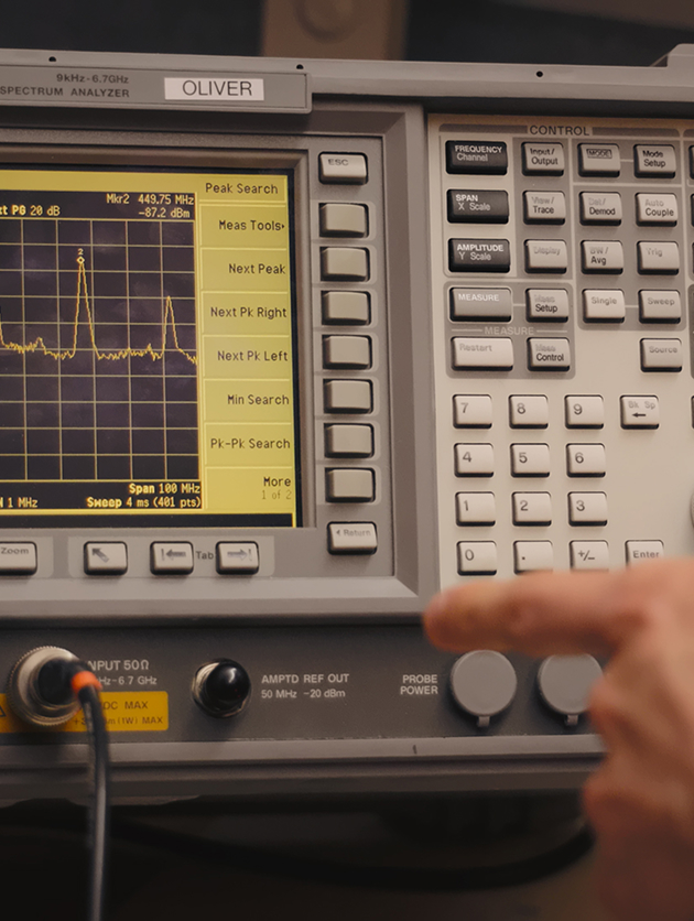
We design custom trace PCB antennas and select off‑the‑shelf antenna solutions based on performance and application needs. Validation is performed in‑house using vector network analyzers, RF signal generators, spectrum analyzers, and a dedicated RF screen room. From the start, our designs account for FCC Part 15, European, and military compliance standards—helping reduce surprises and streamline certification.
Our Design Process
Architecture
We work with you to define a system architecture that meets technical and business constraints.
Schematic and Simulation
Detailed circuit design with SPICE simulation to verify performance before PCB layout.
PCB Layout
Our Cadence Allegro and Altium designers create layouts optimized for signal integrity, EMC compliance, and manufacturability.
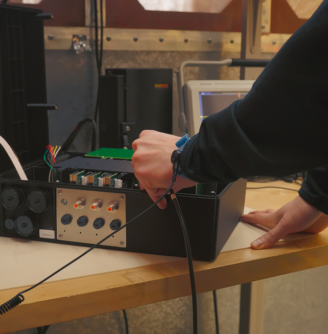
Assembly and Testing
We assemble prototypes in-house using our SMT placement equipment and reflow oven, then test in our electrical labs.
Production Support
We work with your contract manufacturer to ensure successful production, including factory test fixture design.

Tools and Facilities
Electrical design labs equipped with oscilloscopes, spectrum analyzers, specialized RF test equipment, and SPICE for circuit simulation. Multiple Cadence Allegro and Altium PCB design workstations. In-house SMT assembly with machine placement and reflow capability. Test labs including environmental chambers for temperature and humidity testing, a screen cage for RF testing, and a grounded, humidity-controlled lab for electrostatic discharge (ESD) testing.